BITX SSB Transceiver for 14MHz
BITX is an easily assembled transceiver for the beginner with very clean performance.
Using ordinary electronic components and improvising where specific components like toroids are not available, It has a minimum number of coils to be wound.
All alignment is non-critical and easily achieved even without sophisticated equipment. The entire instructions to assemble the rig are given here along with relevant theory.
The Indian hams have often been handicapped by a lack of low cost equipment to get them on air. A mono-band, bidirectional design using ordinary NPN transistors was developed to cater to this demand. The design can be adapted to any particular ham band by changing the RF section coils and capacitors and the VFO frequency.
BITX evolved over one year from the excellent S7C receiver described in the new ARRL book �Experimental Methods in RF Design� (an ARRLpublication) into a bi-directional transceiver. Several hams across the globe contributed to its design. A series of emails were exchanged with OM Wes Hayward (W7ZOI) during the evolution of this design. His contributions have been invaluable. He urged me to strive for higher performance from the simple design. The resultant rig has sensitive receiver capable of strong signal handling, a stable and clean transmitter capable of enough power to make contacts across the World.
All the parts used in BITX are ordinary electronic spares components. Instead of expensive and hard-to-get toroids, we have used ordinary tap washers. Broad-band transformers have used TV balun cores. The entire transceiver can be assembled in India for less than Rs.300. I have designed a single side PCB with large tracks that can be easily etched at home or by any PCB shop. They are also available from OM Paddy, (VU2PEP, pepindia@yahoo.com).
For those who don't read long articles ...
There are a couple of things you should know before you start assembling the circuit:
- The same amplifier block is used throughout. But the emiiter resistors vary in some of the places. Double check the values. If you swap values, the circuit won�t stop working. It will work terribly. That might be a little difficult to diagnose in the end. Check the emitter values and the resistors that go between the base and collector.
- The receiving IF amplifier between the filter and the product detector is coupled to the product detector using a 100pf (not 0.1uf).
- The crystal filter worked for me, I used crystals from the local market marked as KDS. These are the cheapest and they work with the capacitor values given in the filter. Your crystals might require a different set of capacitors. Try the values given here, if you find the bandwidth too narrow, decrease the capacitances, if you find it too open then increase the capacitances.
- The microphone is directly coupled to the amplifier as my headset microphone needs 5V bias. If your microphone works without bias, then insert a 1uf in series with the microphone.
- The pictures show my prototype on two boards. Don�t do that, split up the VFO into a separate box.
- The pre-driver is built onto the main board. The driver and the PA are on a separate board. Keep the same layout to keep the PA stable.
- There is a 50uf on the power line soldered near the BFO, don't forget it. It cleans up the audio noise which would otherwise get into the receiver.
- On the PCB, there are jumpers between T lines and R lines across the ladder filter. There is a jumper from the BFO supply to the VFO suppl


Development Notes
Almost all modes of radio communications share a natural principle that the receivers and transmitters operate using the same line-up of circuit blocks except that the signal direction is reversed. The CW direct conversion transceiver is the simplest illustration of this principle. A more complex example is the bidirectional SSB transceiver.
Bi-directional SSB transceivers have been quite common in amateur literature. A transceiver was described in the ARRL SSB Handbook using bipolar transistors. W7UDM�s design of bidirectional amplifier (as the basis of bidirectional transceiver) is referred to by Hayward and DeMaw in their book Solid State Design. The bidirectional circuitry is often complex and not approachable by the experimenter with modest capability (like me).
The broad band bi-directional amplifier
My current interest in bidirectional transceivers arose after looking at an RC coupled bidirectional amplifier in the book Experimental Methods in RF Design (p. 6.61). An easily analyzed circuit that was simple and robust was required. It began its life as an ordinary broad-band amplifier:
In any bipolar transistor, the current flowing from the collector to emitter is a multiple of the current flowing from the base to the emitter. Thus, if there is a small change in the current flowing into the base, there is a bigger change in the current flowing into the collector. What follows is a highly simplified explanation of working of the above amplifier.
In the above circuit, imagine that a small RF signal is applied through Rin to the base of Q1. Also imagine that the Rf voltage is swinging up. The transistor will accordingly amplify and increase collector current causing more current to flow through the Rl (220 ohms) collector load. This will in turn drop the voltage at the collector. The drop in voltage across the collector will also result in a drop at the base (base voltage is a fraction of the collector voltage due to the way the base is biased). This circuit will finally find balance when the increase in base current flowing from Rin is balanced by the decrease in base current due to the voltage drop across Rl. In effect the RF current entering from Rin flows out through the feedback resistance (Rf). The impedance seen at the base is effectively very low and the signal source will see an approximate input impedance of Rin.
Thus, Vin/Rin = Vout/Rf (Eq.1)
Another factor to consider is that that emitter is not at ground. At radio frequencies, it looks like there is a 10 ohms resistor between the emitter and the ground. Thus, when the base voltage swings, the emitter will follow it. The AC voltage variations across the Re (10 ohms) will be more or less the same as that across the base. The current flowing into the emitter will mostly consist of collector current (and very little base current). Thus, if the emitter current almost equals collector current,
Ie = Vin / Re = Vout / Rl (Eq. 2)
We can combine these two equations to arrive at:
Vout / Vin = Rf / Rin = Rl / Re. (Eq. 3)
This is an important equation. It means several things. Especially if you just consider this part:
Rf / Rin = Rl / Re. (Eq 4)
Let�s look at some interesting things:
- The voltage gain, and the input and output impedances are all related to resistor values and do not depend upon individual transistor characteristics. We only assume that the transistor gain is sufficiently high throughout the frequencies of our interest. The precise value of the transistor characteristics will only limit the upper frequency of usable bandwidth of such an amplifier. This is a useful property and it means that we can substitute one transistor for another.
- The power gain is not a function of a particular transistor type. We use much lower gain than possible if the transistor was running flat out. But the gain is controlled at all frequencies for this amplifier. This means that this amplifier will be unconditionally stable (it wont exhibit unusual gain at difference frequencies).
- You can restate the eq 3 as Rf * Re = Rl * Rin . That would mean that for a given fixed value of Rf and Re, the output impedance and input impedances are interdependent. Increasing one decreases the other and vice versa! For instance, in figure 1, Rf = 1000, Re = 10, if we have Rin of 50 ohms, the output impedance will be (1000 * 10)/50 = 200 ohms. Conversely, if we have an Rin of 200 ohms, the output impedance will be 50 ohms!
In order to make bidirectional amplifiers, we strap two such amplifiers together, back to back. By applying power to either of amplifiers, we can control the direction of amplification. This is the topology used in the signal chain of this transceiver. The diodes in the collectors prevent the switched-off transistor�s collector resistor (220 ohms) from loading the input of the other transistor. A close look will reveal that the AC feedback resistance consists of two 2.2K resistors in parallel, bringing the effective feedback resistance to 1.1K. Thus, the above analysis holds true for all the three stages of bidirectional amplification.
Diode mixers
The diode mixers are inherently broadband and bidirectional in nature. This is good and bad. It is good because the design is non-critical and putting 8 turns or 20 turns on the mixer transformer will not make much of a difference to the performance except at the edges of the entire spectrum of operation.
The badness is a little tougher to explain. Imagine that the output of a hypothetical mixer is being fed to the next stage that is not properly tuned to the output frequency. In such a case, the output of the mixer cannot be transferred to the next stage and it remains in the mixer. Ordinarily, if the mixer was a FET or a bipolar device, it usually just heats up the output coils. In case of diode ring mixers, you should remember that these devices are capable of taking input and outputs from any port (and these inputs and outputs can be from a large piece of HF spectrum), hence the mixer output at non-IF frequencies stays back in the mixer and mixes up once more creating a terrible mess in terms of generating whistles, weird signals and distorting the original signal by stamping all over it.
A simple LC band pass filter that immediately follows the diode ring mixer will do a good job only at the frequencies it is tuned to. At other frequencies, it will offer reactive impedance that can cause the above mentioned problems. It is requirement that the diode mixer�s inputs and outputs see the required 50 ohms termination at all the frequencies. In other words, they require proper broadband termination. Using broad-band amplifiers is a good and modest way of ensuring that. A diplexer and a hybrid coupling network is a better way, but it would be too complex for this design.
Circuit Description
Although simple, every effort was made to coax as much performance as was possible given the limitations of keeping the circuit simple and affordable.
The Receiver
The RF front-end uses a triple band-pass filter for strong image and IF rejection. The three poles of filtering are quite adequate and the out-of-band response of the receiver is only limited by external shielding and stray pickups.
An RF amplifier follows the RF band pass filter (Q1) biased for modest current. More current would have required a costlier transistor. There is 8mAs through the RF amplifier and the post-mix amplifiers to keep the signal handling capacity of the circuit above average. The Post-mix amplifier (Q2) does the job of keeping the crystal filter as well as the diode mixer properly terminated. The crispness of the receiver is more due to this stage than anything else. An improper post-mix amplifier easily degrades the crystal filter�s shape and introduces spurious signals and whistles from the diode mixer. Note that the mixer is singly balanced to null out the VFO component and not the RF port and in the absence of proper pre-selection, 10MHz signals can easily break into the IF strip.
The VFO is fed via a broad-band amplifier into the singly balanced mixer. We used the simplest VFO possible with a two-knob tuning mechanism. It works really well and for those (like me) used to quick tuning, it offers best of both worlds, slow tuning through the varactor and fast tuning through the capacitor without any slow motion drive. Getting a slow motion drive is an increasingly difficult problem and this is an �electrical� substitute for slow motion drives.
A word about the VFO: depending upon component availability, skills and preferences, everybody has a favourite VFO circuit. Feel free to use what you have. Just keep the output of the collector of Q7 to less than 1.5 volts (it will appear clipped on the oscilloscope trace, that is okay). For 20 Meters operation, you will need a VFO that covers 4 to 4.4MHz. The given VFO has low noise though it does drift a little, but I have had no problems with ordinary QSOs. After 10 minutes of warm up, the drift is not noticeable, even on PSK31 QSOs.
A Hartley oscillator using a FET like BFW10 or U310 would work much better. You can substitute this VFO with any other design that you might want to use. If you are using the PCB layout, then skip the VFO on board if you want to use a different VFO and build it externally in a separate box.
The simple IF amplifier has a fixed gain. Earlier it was noted that IF amp was contributing noise at audio frequencies. It was later traced to noise from the power supply and placing a 50uf on the transceiver power line has cured it. The IF amplifier has a 100pf output coupling to provide roll-off at audio frequencies.
The BFO is a plain RC coupled crystal oscillator with an emitter follower. The emitter follower has been biased to 6V to prevent limiting.
The detector also doubles up as the modulator during transmit mode; hence it is properly terminated with an attenuator pad. It has no impact on the overall noise figure as there is enough gain before the detector. The audio pre-amplifier is a single stage audio amplifier. The 220pf capacitor across the base and collector provides for low frequency response.
The receiver does not have an AGC. This is not a major short-coming. Manual gain control allows you to control the noise floor of the receiver and I personally find it very useful when searching for weak signals or turning it down to enjoy the local ragchew.
Transmitter
The microphone amplifier is DC coupled to the microphone. This was done to steal some DC bias that is required when using a Personal Computer type of headset. If your microphone does not require any bias, then insert a 1uF in series with the microphone. The microphone amplifier is a simple single stage audio amplifier. It does not have any band pass shaping components as the SSB filter ahead will take care of it all. One 0.001uf at the microphone input and another at the modulator output provide bypass for any stray RF pickup.
The two diode balanced modulator uses resistive as well as reactive balancing. A fixed 10pf on one side of the modulator is balanced precisely by a variable 22pf on the other side. A 100 ohms mini preset allows for resistive carrier balance. The attenuator pad at the output was found necessary to properly terminate the diode modulator and keep the carrier leakage around the IF amplifier to a minimum. While this may seem excessive, it produces a clean DSB with carrier nearly 50db down with careful adjustments on the oscilloscope.
Rest of the transmission circuitry is exactly the same as the receiver. There is an extra stage of amplification (Q14) to boost the very low level 14MHz SSB signal from output of the microphone tip to driver input level.
The output amplifier boosts the SSB signal to 300mV level, enough to directly drive a driver stage.
The Power Chain
A simple power chain consisting of a low-cost medium power NPN transistor (2N2218) driving an IRF510 for 6 watts of power at 14MHz. The output of IRF510 uses a tap washer as an output transformer. The output transformer has 40 turns of bifilar winding; these can lead to enough stray capacitance to affect proper performance as a transformer. The half-wave filter that follows the transformer absorbs these capacitances as a part of the matching network.
I used this power chain because it works for me and delivers 6 watts on 14MHz. I don�t use more power because I neither require more nor do I have a power supply that can source more. If you need more power, there are a number of things that you can do, you can simply increase the supply voltage on the IRF510 up to 30 volts and extract nearly 15 watts of power from the same configuration. At 30 volts, the drain output will be at 30 ohms impedance and the pi-network will have to be designed to directly match the drain to a 50 ohms antenna load. Alternatively, you could try two IRF510s in push-pull. These are variations that you can play with. A word of warning though, The RF energy at these levels can give you a serious RF burn. RF burns can be more painful than fire or steam burns. QRP is not only fun, it is also safe.
Construction
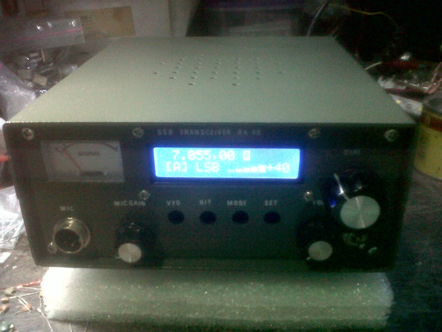
I would highly recommend that you construct it over a plain copper clad board by soldering the grounded end of the components to the copper and the other ends of components to each other. Look at the pictures to see how it has been done. If you don�t know about this method of assembling RF circuitry, then you should read about it, there are quite a few write ups on the Internet about this method of RF experimentation. It does not require any PCB, it is quite robust and very stable.
Assembling the PCB
For those who feel intimidated by this �ugly� method, I have designed a PCB. The PCB layout (component side) is provided with this article. It is a single sided PCB with wide tracks that can be easily made in the home lab. I am making a run of these PCBs but shipping them abroad (outside India) maybe a problem. Drop a mail to me if you are planning to make some PCBs, I can put your contact information on the website. There are no copyrights over either the PCB, the circuit or even this article, feel free to copy and distribute.
The PCB is laid out in a long line.It is 8-1/2 inch long and 2-1/2 inch wide. The circuit board is big for the circuit that goes onto it. This was done so that the board is non-critical and it works well. All the bidirectional amplifiers are similarly laid out.
When you get your PCBs, inspect them thoroughly, preferable in the Sun. Check for small cracks in the tracks. Check for tracks that might be touching each other or touching the ground plane. The PCB layout was done to minimize this, but check it anyway. Especially check for the tracks that run diagonally to the base of each transistor in the bidirectional circuitry. These are laid out very closely and they are candidates for shorting.
Almost all assembly instructions ask you to solder the transistors in the end. I would highly recommend that you solder the transistors and the diodes first. You are most alert when you start a project and if you place the transistors correctly, the rest of the circuit can be soldered around it. Be very careful about the orientation of each transistor. The microphone amplifier transistor (Q10) faces in a direction opposite to the rest of the transistors and the transistor pairs in bidirectional amplifiers face each other. The diodes have a ring to indicate which way their �arrow� is pointing.
After the transistors are soldered, finish the BFO. If you are assembling this for 14MHz and above, the BFO will need a coil in series with the crystal (USB mode), if you are need LSB operation, you will need a trimmer instead (see the schematic). Apply power to the BFO and you should be able to hear it on your Short wave broadcast radio around 31 meter band. It will sound like a silent radio station. It should be quite strong. Switching the BFO power supply on and off will help you identify your BFO signal on the radio. If you have an RF probe, or an oscilloscope, you should be able to see the oscillations. Expect RF of 2 volts or more.
Next, assemble the VFO. Winding 150 turns of the VFO coil is one of the most tedious jobs while assembling this rig. It has to be done, so just dig in and do it. You don�t have to attach the 365 pf tuning capacitor yet. Check the oscillations on a receiver or a frequency counter. You may have to decrease the number of turns. Without the 365 pf, the 22pf trimmer should be able to set the VFO to 4.3MHz or so. If the VFO is oscillating at a lower frequency, then remove some turns from the coil. If the VFO is at a higher frequency, add 22pf in across the 22pf trimmer (if you are using the PCB, solder in from the foil side). You will require a wire jumper to carry power supply between the VFO and the BFO. They are the only stages that remain switched on during both transmit and receive.
Assemble the audio pre-amplifier and the audio power amplifier and attach the volume control. When power is applied to the audio stages, touching a finger to the base of Q4 should produce static in the speaker to move even the most die-hard trash metal rockers.
Next, assemble all the three bi-directional stages! This involves lot of soldering. But all the six stages are exactly the same. Finish one stage at a time. The capacitors are symmetrically laid out and all of them are 0.1uF with one exception (100pf at the output of Q3). Remember that the emitter bias resistors are 100 ohms, 220 ohms or 470 ohms. If you mix up the values, the rig will still work but it will under perform in the presence of strong signals and the transmission will be splattered. There are jumpers for T and R line across the crystal filter. Solder them up and power on the R line and then the T line alternatively. The emitters of bidirectional stages should show 2 volts approximately and the collectors should show around 8 volts and the switched-off transistor should show zero voltage on all the three leads.
For the moment of truth, solder the three coils, trimmers and capacitors of the RF filter, attach an antenna and switch it on! Check that the stages are working starting from audio end. If you touch the volume control�s control pin, you should hear AC hum and static. If you touch the base of Q4, there should be a pretty loud static. Take a lead from your VOM and touch Q3, you should get very loud static, probably mixed with local AM broadcast. Touch the base of Q2 with the test lead and you should get lesser static as the filter allows only 3 KHz of 10MHz through.
Finally, connect the antenna properly at the input of the RF band-pass filter and peak up the three trimmers for maximum atmospheric noise. Attach the 365 pf and start tuning around the band, peak the RF front-end on a strong signal and then tune in a weaker signal and peak for maximum clarity (not maximum sound).
An important note: Be sure that you have connected a proper 50 ohms antenna load. The RF filter performs correctly only at 50 ohms. If you use a long wire to do the initial testing, you will have to touch up the trimmers again for the proper antenna.
Take a break, spend the evening listening to your new homebrew. If the CW signals tune to dead beat and rise on the other side again, your BFO has to move its frequency. For USB, add more turns to the coil to the BFO coil, for LSB, tweak the trimmer. You should have a perfect single signal reception. If you tune past the dead-beat of a CW signal, the signal should drop out completely.
Assembling the microphone amplifier (Q10) and the output amplifier (Q14) will complete the exciter portion of the transceiver. To put the transceiver in transmit mode, ground the R line and apply 12V on the T line. Attach the output of Q14 to an oscilloscope but don�t attach the microphone yet. Null the carrier with the 100 ohms preset and the 22pf trimmer. Each affects the other so you might have to go back and forth between the two controls.
Now plug-in the microphone and speak into it. You should be able to see clean SSB of between 200 and 300 mV on the scope at the output of Q14. Instead of the oscilloscope you can use another 14MHz receiver to test your transmission quality. Switch off the AGC of the other receiver while setting the carrier null. A soft whistle (if you can manage) into the microphone is should result in a full carrier at the output.
Next, assemble the power chain. At this point, you will need a suitable chassis to house your project. Any metal box will do. If you don�t have any, you can solder pieces of copper clad together (like I did) and make a U shaped chassis. Keeping the VFO in open air makes it drift a bit. A closed box is really very useful.
A big cookie (or chocolate) box of tin is really ideal. With a hand drill, you can easily make holes to fit the two PCBs inside it. Tin is easily soldered on. Use the biggest knob you can find for the main tuning. The plastic broadcast capacitors usually have a very short stub that cannot take a big knob. It takes on a small plastic drum that is held onto the capacitor spindle with a retaining screw. Clip on the drum onto the tuning capacitor, tighten the retaining screw well and with epoxy glue, stick a big knob over the drum. This will make your main tuning mechanism.
I use a simple double pole triple throw switch for Transmit/Receive switch-over. If you prefer PTT operation, you can easily substitute the switch for a relay. Be sure to solder a reverse biased diode across the relay coil to prevent reverse voltage from entering into the transceiver power line.
Use shielded cable for all the connections between the power amplifier and the main board.
Tune-up and Operation
Set the VFO to correctly cover 4.0 to 4.4MHz. If you can, take your rig over to a ham friend�s shack, you can monitor your VFO on his rig at the edge of 80 meters band at 4.0MHz. Set the trimmer so that you can hear the VFO when the friend�s receiver is tuned to 4.0MHz and your tuning capacitor is fully closed (as much as it will go anti-clockwise). After this, connect the antenna and peak the RF coils for maximum noise in the speaker. If you can tune it to a weak signal, then peak the RF coils for best reception.
You might find that although you are able to tune in CW stations, you are unable to hear the SSB stations properly. This indicates that your BFO is not properly set. We will take that up next.
On amateur bands above 10MHz, SSB is transmitted on upper sideband and on bands below 10 MHz, it is transmitted on lower sideband. To tune a upper side-band signal, your BFO has to be at the lower edge of the crystal pass-band. You will require either the inductor (for USB) or the capacitor (for LSB) in series with the BFO crystal. If your BFO is set to proper frequency then the signals will tune in and as you continue tuning across the signal, they will drop in pitch and disappear. If the signals appear muffled, then the BFO is set in the crystal filter�s center, add more turns to the coil (USB), or tweak the trimmer (LSB). If the signals appear shrill and you are unable to zero-beat them, then the BFO is too far away from the filter�s frequency - Decrease the coil�s turns (for USB) or tweak the trimmer (LSB).
The transmitter tune-up essentially involves setting the carrier null. It is best to tune up the transmitter on a dummy load. I use 8 220 ohms, 2 watts resistors in parallel as my dummy load. It is worth the few bucks to have a proper dummy load. Attach the dummy load on the transmitter, and attach an RF probe to the dummy load (or an oscilloscope). As you speak, you should get 20 volts or more peak voltage on the dummy load when you whistle or just go �haaaaallow�. On another receiver in the same room, connect a short piece of wire as an antenna and monitor your own signal. You will probably be able to hear your own carrier as well. Null it by tweaking the 100 ohms preset and the 22pf balance trimmer. They both interact, so you might have to go back and forth between the two controls.
A word of caution, the diode mixers are prone to generating odd harmonics. The third harmonic of 4 MHz is at 12MHz. So, if you simply peak the coils for maximum output on transmit, you might wrongly peak the RF front-end to 12 MHz (I did that). The RF band-pass filter is best tuned in receive mode over a weak signal at 14.150MHz or so and left at that.
Conclusion
There might be a kit (components and the PCB in a bag) soon. I personally don�t have the time to put kits together. If somebody is interested in doing so, just go ahead and do it. The design is free, you don�t need to ask my or anybody else�s permission. If you can drop me a line, I will list you as a kit supplier on my site.
This is also the first time I have put out a PCB design for my rig. The purpose is to address the need among Indian hams in particular for an SSB rig that is easily and cheaply built. My original aim was to keep the price under Rs. 1000. The current design brings the cost to well under Rs.300 (less than 7 dollars). Contact OM Paddy (VU2PEP) for the PCBs. His email is pepindia12345@yahoo.com (I have added �12345� to confuse programs that automatically gather email addresses from my site, there is just �pepindia� before the at sign).